Lab 1
Introduction
The purpose of Lab1 was to assemble the PCB, establish a connection to the FPGA and MCU, and write a simple program to drive three LEDs as well as a seven-segment display simultaneously using four input switches.
Schematic
The circuit diagram to drive the three LEDs and the seven-segment display using four input switches is as follows: 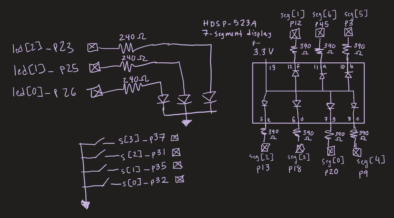
The calculations for the current draw of the seven-segment display are: 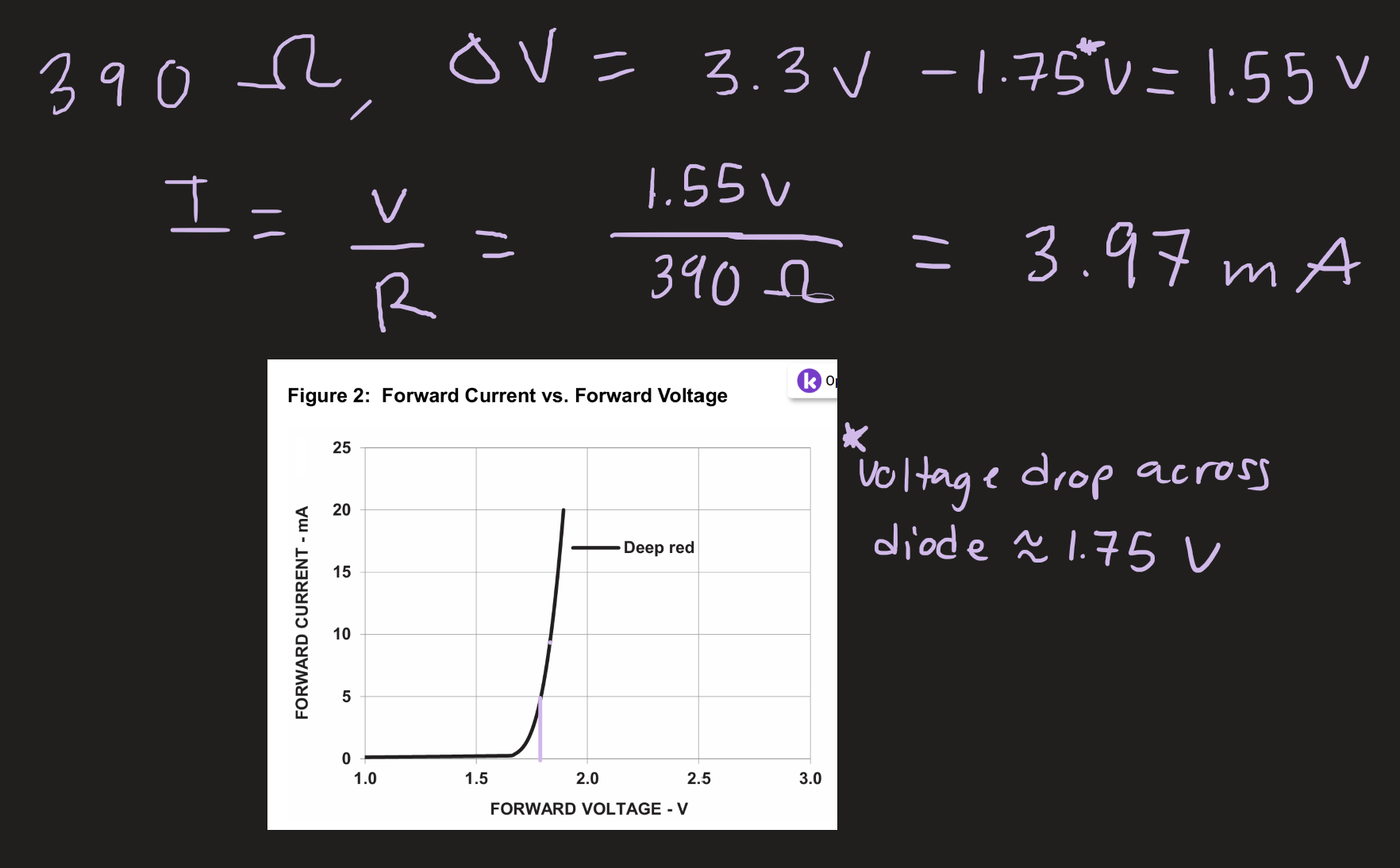 This is because the seven-segment display is being powered by 3.3V, and each diode within the display experiences a voltage drop of 2V. The resistor values of 330 Ohms I chose resulted in a current draw of 3.93 mA, which is less than the recommended range of 5mA-20mA, but the diodes still shone visibly while remaining well under the maximum allowed current of 20 mA. While different from what I ended up doing, 100 Ohm resistors could be used to yield a current of (1.3V/100 Ohms) = 13 mA, which is within the recommended operating range of the 7-segment display.
Block Diagram
The block diagram of the systemverilog code is: 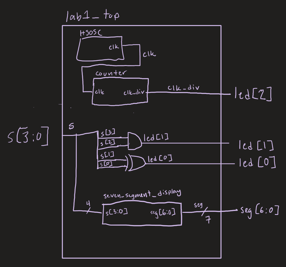
Code
The systemverilog code itself is:
/*
lab1_top.sv

Drives three LEDs and a 7-segment display based on inputs from
four switches. 7-segment display counts up from 0-F in hex based
on the binary value encoded by the state of the switches.
The first LED is lit when the first two switches are pushed simulateously.
The second LED is lit when the third XOR the fourth switch is pulsed.
The third LED pulses at ~2.8 Hz.

Madeleine Kan
mkan@hmc.edu
3 September, 2025
*/

module lab1_top(
    input logic [3:0] s,
    output logic [2:0] led,
    output logic [6:0] seg
);
    logic clk_div;
    logic [6:0] seg_out;
    // Internal high-speed oscillator
    HSOSC #(.CLKHF_DIV(2'b01)) // 24MHz from clk divider
     hf_osc (.CLKHFPU(1'b1), .CLKHFEN(1'b1), .CLKHF(clk));

    // Counter
    counter count(clk, clk_div);

    // 7-segment display
    seven_segment_display display(s, seg_out);

    // Assign LED output
    assign led[0] = s[0] & s[1];
    assign led[1] = s[2] ^ s[3];
    assign led[2] = clk_div;
    assign seg = seg_out;

endmodule

/*
counter.sv

Takes in clk, clock signal
Outputs clk_new, a new clock signal that rises every 2^23 clk cycles
Madeleine Kan
mkan@hmc.edu
3 September, 2025
*/

module counter
     (input logic clk,
     output logic clk_new);

    logic [23:0] counter;
    always_ff @(posedge clk)
        counter <= counter + 24'b1;
    assign clk_new = counter[23];
endmodule

/*
seven_segment_display.sv
Drives HDSP-521A Seven-Segment Display
with common anode (meaining diodes are
pulled to ground to activate)
Madeleine Kan
mkan@hmc.edu
3 September, 2025
*/

/*
seven_segment_display.sv
Drives HDSP-521A Seven-Segment Display
with common anode (meaining diodes are
pulled to ground to activate)
Madeleine Kan
mkan@hmc.edu
3 September, 2025
*/

module seven_segment_display(
    input logic [3:0] s,
    output logic [6:0] seg
);
    always_comb
        case(s)
            //                abcdefg
            4'b0000: seg = 7'b0000001; // 0
            4'b0001: seg = 7'b1001111; // 1
            4'b0010: seg = 7'b0010010; // 2
            4'b0011: seg = 7'b0000110; // 3
            4'b0100: seg = 7'b1001100; // 4
            4'b0101: seg = 7'b0100100; // 5
            4'b0110: seg = 7'b0100000; // 6
            4'b0111: seg = 7'b0001110; // 7
            4'b1000: seg = 7'b0000000; // 8
            4'b1001: seg = 7'b0001100; // 9
            4'b1010: seg = 7'b0001000; // a
            4'b1011: seg = 7'b1100000; // b
            4'b1100: seg = 7'b0110001; // c
            4'b1101: seg = 7'b1000010; // d
            4'b1110: seg = 7'b0110000; // e
            4'b1111: seg = 7'b0111000; // f
            default: seg = 7'b1111111; // none
        endcase
endmodule
The scratchwork to develop the truth table for the seven_segment_display module was: 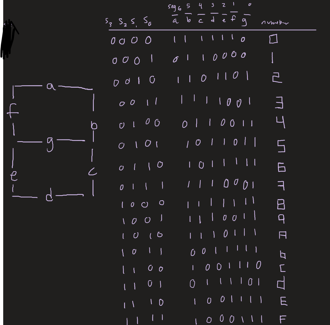
Results
The design met all intended design objectives, as verified by the following QuestaSim simulations:
lab1_top testbench 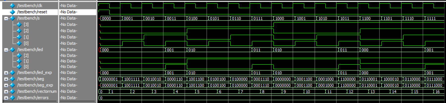
seven_segment_display testbench 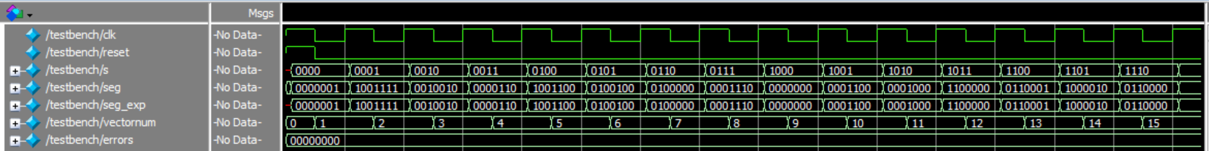
As we can see, all of the testvectors passed the testbenches, demonstrating intended funcitonality of both modules.
This lab took me around 20 hours.
Reflection
Reflection before lab regrade:
This lab met all but one proficiency requirement, as specified in the Lab 1 spec sheet. The missing proficiency requirement is due to the missing 5V regulator and SMT diodes, which were not available in the digital lab at the time of completion. I will find and solder these on during the next week.
In terms of the excellence requirements, I provide calculations to show how to maintain the current draw in each diode of the seven-segment display within the recommended operating conditions of 5-20 mA. However, this differs slightly from what I ended up doing. This is because I noticed that the 3.3V output from my PCB was not working as intended; originally, it was outputting 1.4 V instead of 3.3V. I worked with Abe to attach a 3.3V regulator, but then the output started yielding <1V. During this time, I decided to supply the seven-segment display with 5V, thus necessitating the higher resistor value. Later, I moved the entire circuit from the PCB to the breadboard, so I was able to use the 3.3V power source again. However, since I was limited on time, I did not change the resistors back from 330 Ohms to ~100 Ohms. Next week, I will be sure to start the lab earlier and schedule more time to work on it so I can perform more thorough organized work.
The other excellence requirement I did not meet was the QuestaSim automatic testbench requirement. I started working on a testbench and testvector for seven_segment_display.sv, but I ran into difficulty with reading in the test vectors, and I unfortunately ran out of time to debug this.
While I didn’t get to complete automated testbenches myself before the check-in time, I did help some peers debug their testbenches, and I have a sense of how I would approach simulating my code for future labs.
Reflection post updating lab for regrade
This lab meets all proficiency and excellence specifications. The main issues I ran into were as follows:
Hardware issues with the 3.3V regulator
Firmware issues; I forgot to (re)set the top-level module, so the 3 led pins ended up not being driven. This could be seen in the pin assignment window. Since the pins weren’t being driven, they were at 3.3V as a default, but this voltage dropped to 1.8V when the pin was connected to the LED. To fix this, I had to go under the project menu and set the appropriate module as the top-level module and resyntesize.
The testbench couldn’t read the testvector file; this was remedied by referencing the absolute path of the testvector file (rather than the relative path).
AI Prototype
I gave ChatGPT this prompt:
LLM prompt Write SystemVerilog HDL to leverage the internal high speed oscillator in the Lattice UP5K FPGA and blink an LED at 2 Hz. Take full advantage of SystemVerilog syntax, for example, using logic instead of wire and reg.
It generated the following code, accompanied by a high-leve overview of how the clk frequency is customized:
module led_blinker (
    input logic clk,      // High-speed clock (e.g., 12 MHz)
    output logic led      // LED output (blinking at 2 Hz)
);

    // Define a parameter for clock frequency and target frequency for blinking
    parameter integer HIGH_SPEED_CLK_FREQ = 12000000;  // 12 MHz internal oscillator
    parameter integer TARGET_FREQ = 1; // 1 Hz (for 2 Hz blinking)

    // Calculate the division factor (this depends on the input clock and target frequency)
    localparam integer DIVIDE_FACTOR = HIGH_SPEED_CLK_FREQ / (TARGET_FREQ * 2); // Divide by 2 for full period

    // Counter to divide the clock frequency
    logic [31:0] counter;  // Counter to keep track of clock cycles

    // Clock divider and LED toggle logic
    always_ff @(posedge clk) begin
        if (counter < DIVIDE_FACTOR - 1) begin
            counter <= counter + 1;
        end else begin
            counter <= 0;
            led <= ~led; // Toggle LED state on every period of the divided clock
        end
    end

endmodule
The code did synthesize on the first try, which was good, and the description would have been helpful if customizing the frequency of a clock signal in system verilog was completely new to me. However, one issue is that ChatGPT hardcoded the internal clk frequency, and it didn’t actually interface with the Lattice UP5K HSOSC. It also did not include any resources where users could find information about the Lattice UP5K HSOSC, like the official documentation. Additionally, it doesn’t really talk about how the size of the counter vector (N) or the constant that is added to counter every clock cylce (p) can be adjusted to derive a desired clock frequency–it basically assumes that the only way to create a clock signal with a desired frequency is to find an internal clock that is already some power of 2 of that frequency. When I was writing the code to get an LED to blink at 2.4 Hz, I found reading the documentation for the HSOSC, referencing the formula for f_PWM from the E85 textbook, and referencing my old E85 code to be the most helpful. All three of these resources provided valuable information not covered by ChatGPT’s first response. If I were to use AI in my workflow, I would try to research what I’m trying to accomplish so that I can tune my prompt to get more valuable and detailed information.
Reference
Code can be found in this github repository